Advanced Photolithography Systems
The LIMA Lithography Systems are designed specifically for patterning and lithography requirements in semiconductor device manufacturing. With a user-friendly interface and low infrastructure costs, these systems deliver high-quality lithography results comparable to international platforms while maintaining ease of use and accessibility for both R&D and production environments.
System Configurations
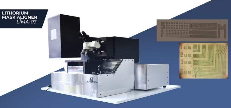
LIMA-04
Designed for samples from 10×10 mm up to 4-inch wafers
Alignment via microscope and camera options
Custom-designed homogeneous illumination optical system
Semi-automatic motorized alignment using joystick control
Electromechanical WEC (Wedge Error Compensation) system
Compatible with soft, hard, and brittle substrates
LIMA-06
Industrial semi-automatic 6-inch photolithography system
User-Friendly Design: Intuitive interface with minimal training required
Low Infrastructure Cost: Efficient system design reduces setup expenses
High-Quality Results: Comparable to international platform standards
Flexible Configuration: Suitable for various substrate sizes and types
Reliable Performance: Proven technology for consistent lithography results
LIMA Lithography Systems
Advanced photolithography technology for semiconductor device manufacturing. Contact us for technical consultations and system demonstrations!
SPECIFICATION
LIMA-04
LIMA-06
SUBSTRATE SIZE
10×10 mm to 4 inch
10×10 mm to 6 inch
EXPOSURE AREA
120 × 120 mm
160 × 160 mm
ILLUMINATION UNIFORMITY
< 3%
UV SOURCE
UV-LED (365 nm / 405 nm)
ALIGNMENT METHOD
Microscope & Camera
Dual-sided Microscopes
ALIGNMENT CONTROL
Semi-automatic (Joystick)
Semi-automatic (Joystick & Touchscreen)
WEC SYSTEM
Electromechanical
Pneumatic
CONTACT MODES
Hard / Soft / Proximity
RESOLUTION (UV300)
<1 µm (Hard), <2 µm (Soft), <4 µm (Proximity)
SUBSTRATE COMPATIBILITY
Soft, Hard, Brittle substrates
System Features
OPTICAL SYSTEM
Custom-designed homogeneous illumination
UV-LED technology for reliable exposure
Compact design replacing traditional Hg lamps
<3% illumination uniformity across exposure area
ALIGNMENT SYSTEM
LIMA-04: Microscope and camera alignment options LIMA-06: Dual-sided independently movable alignment microscopes
Semi-automatic motorized alignment with joystick control
High-precision positioning for critical alignment
CONTACT CONTROL
LIMA-04: Electromechanical WEC system LIMA-06: Pneumatic WEC system
Multiple contact modes: hard, soft, proximity
Compatible with various substrate types
USER INTERFACE
Intuitive control interface LIMA-06: Additional touchscreen control
User-friendly operation with minimal training
Low infrastructure requirements
APPLICATIONS
MEMS, LED/Laser devices, photodetectors, transistors
Electronic devices, cameras, microfluidic channels
Microbiology applications, lab-on-a-chip systems
Semiconductor device manufacturing and R&D
Model Selection Guide
LIMA-04: Ideal for laboratory and R&D applications with 4-inch wafer capability. Features electromechanical WEC system and joystick control for precise alignment.
LIMA-06: Industrial semi-automatic system for 6-inch wafers. Enhanced with dual-sided alignment microscopes, touchscreen interface, and pneumatic WEC for production environments.
Note: LIMA Lithography Systems provide advanced photolithography capabilities with user-friendly design and low infrastructure costs. Contact us for detailed specifications, demonstrations, and customization options.