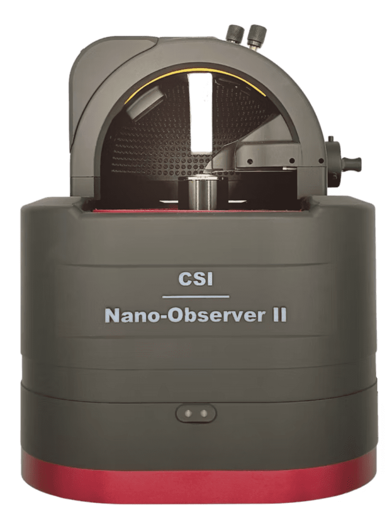
Nano-Observer II
Advanced Atomic Force Microscope — Nano-Observer II
The Nano-Observer II is a cutting-edge Atomic Force Microscope (AFM) manufactured by CSInstruments (France), combining flexibility, exceptional performance, and user-friendly operation. It features proprietary technologies — ResiScope™ for 10-decade electrical range, HD-KFM for artifact-free surface potential mapping, and Soft-IC for zero-friction measurements on delicate samples. Designed for both advanced users and beginners, it offers 15+ AFM modes on a single, upgradable platform.
Key Applications
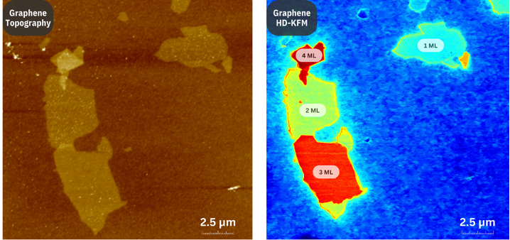
- Semiconductor and 2D materials research (graphene, hBN, MoS₂)
- Energy materials — battery electrodes, photovoltaics, fuel cells
- Polymer and composite characterization
- Thin film and coating analysis
- Biomaterials and life science research
- Piezoelectric and ferroelectric materials
- Failure analysis and quality control
Essential Features
ResiScope™ — 10-Decade Range
Measures 10² to 10¹² Ω and current from fA to μA in a single scan — no gain switching, no saturation. Real-time adaptive electronics for artifact-free current/resistance maps.
HD-KFM — Artifact-Free KPFM
Single-pass surface potential mapping using the cantilever’s second eigenmode (~350–400 kHz). Eliminates topographic artifacts of standard lift-mode KPFM with sub-10 nm resolution.
Soft-IC (Soft Interaction Control)
Pixel-by-pixel measurement with zero lateral contact. Enables quantitative electrical, thermal, and piezo measurements on delicate samples without damage.
24-bit USB AFM Controller
Low-noise electronics with integrated digital lock-in up to 6 MHz. Intuitive AutoScan software with automated approach and real-time active gain control.
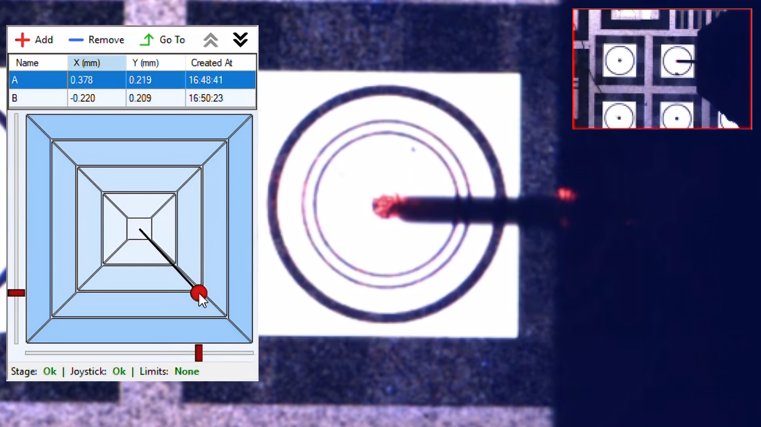
Motorized Stage Option
Built-in motorized stage for large-sample mapping, statistical multi-site analysis, and high-throughput workflows. Point, click, and measure automatically.
25 × 25 mm travel
Glovebox Compatible
Compact design enables full operation inside a glovebox for air-sensitive materials — battery electrodes, perovskites, organic electronics.
AFM-IR Nano-Spectroscopy
Open design for coupling with IR laser sources. Sub-100 nm chemical mapping — correlate topography, electrical, and chemical data on the same sample area.
All Available Modes
Resonant / Tapping
Soft-IC
ResiScope™
Soft-ResiScope™
HD-KFM
Kelvin Force (double-pass)
Electrostatic Force
C-AFM
Scanning Microwave Impedance
PFM
MFM
Soft-MEKA
Force Modulation
Nano-Indentation
Force Spectroscopy
Phase
LFM
Environmental Options
🌡 Peltier / Heating Stage
🔬 SThM
💧 Liquid Cell
⚗ Electrochemistry
💨 Gas / Humidity Control
🔴 AFM-IR (UV, IR, Raman)
Application Notes
Real scan results published by CSInstruments — the same materials and challenges encountered in leading research labs.


Why Choose the Nano-Observer II?
- Unmatched Electrical Range: ResiScope™ delivers 10² – 10¹² Ω in a single scan — far beyond standard C-AFM
- True Surface Potential: HD-KFM provides artifact-free, single-pass Kelvin Probe measurements
- Gentle on Delicate Samples: Soft-IC enables zero-friction electrical, thermal, and piezoelectric measurements
- Automated Large-Area Mapping: Motorized stage with 0.5 µm resolution and 25 × 25 mm travel for high-throughput workflows
- Versatile Platform: 15+ AFM modes on a single, upgradable system — mechanical, electrical, magnetic, and environmental
- Glovebox Ready: Full AFM capability inside controlled atmosphere environments
- Open Design: Integration with optical microscopy techniques (UV, IR, Raman) and AFM-IR nano-spectroscopy
- Trusted Worldwide: Used at CNRS, Toyota, IBM, TotalEnergies, Max Planck Institute, and leading research institutions
Available Through Utrecht Instruments
Contact us for a demonstration, technical consultation, or competitive pricing on the Nano-Observer II AFM.